

Presentation
About
My name is Andrianakis Haris i come from Greeceand i'm an Electronic Computer Systems Engineer
This is a project i designed on 2010 but never had the time to build and test. After my bachelor degree on Electronic Computer Systems Engineering i found some spare time where i managed to send the pcb layout for manufacturing and test it.
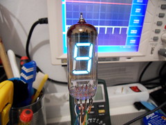
Everything started when i came across with a set of six IV-11 vfd tubes, i ordered from a Russian seller.I found very impressive their retro style as well as the fluorescent color of each segment. While i was thinking what i could do with these tubes i found some real time clocks on the internet which i really liked. I decided that it could be a good idea to design and built my own for my home.
And... the adventure began
Design
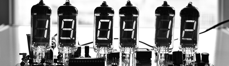
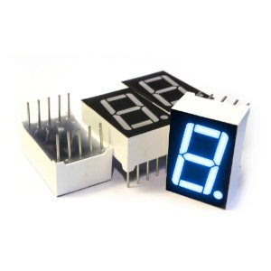
For those who don't have any idea what a VFD Tube is. A VFD Tube is the old style of todays LED 7-segment displays you find on alarm clocks and in most digital domestic appliances.
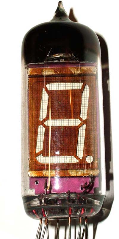
The way they work looks similar to the way the LED 7-segments work with some differences.
- The Filament. VFD tubes have 2 more pins for the Filament which are need to power the tube (like VCC and GND on a chip). These two pins according to the Datasheet needs to be supplied with 1.2Volt and nothing more (polarity doesn't matter).
- The Grid. The Grid is like the common anode of a LED 7-Segment display. So the Grid has to be pushed to high state at 60Volt in our case.
- The Segments. The Segments works like LED segments. They light up simple by pushing them high at 60Volt.
Powering the tubes manually
To do the powering of the tube digitaly and use it in the final design we have to built a simple circuit which will drive the above voltages with digital signals (0-5V). The circuit has to be able to push each segment at 60Volt or Pull it to Ground at 0Volt. To do this two transistors (Push-Pull) are need for each segment. One for pushing the voltage and one for pulling it down.
Push Pull Transistor connection:

There are 10 lines at each tube which need push pull transistors including Dot segment and Grid. So we have 2 transistors x 10 lines= 20 transistors in total for one tube, 30 for 6 tubes (8 lines for segments are in common for all tubes, only Grid is seperate and used for multiplexing). The number of transistors needed are enough for a fault on soldering or pcb etching (more routes) decreasing the finall product reliability and increasing the cost.
To make VFD tube driving easier and more reliable Maxim has built MAX6921. This chip is a Push Pull shift register where each bit of the register is ported on a specific pin of the device. When we shift a set bit (1) the corresponding pin will be pushed high and if we shift '0' the corresponding pin will be pulled low. The communication to the shift register is implimented via SPI which makes it more easier to connect as most of the MCU's nowadays have embedded SPI. By using this chip we only need 3 pins from the main MCU to impliment the SPI communication and nothing more.
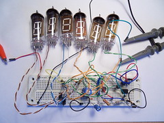
Prototyping and the basic powering circuit using MAX6921 VFD tube driver.

To make all 6 tubes used in this clock, to display at the same time it is need to multiplex them. To do so each tube has to be turned on and off in the row, more than 30 times per second (>30hz) in order, the transaction not to be visible to the human eye. As you can see on the above up right video multiplexing for two tubes is tested.
Testing Filaments in series.
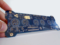
The final circuit.
The main brain of the device has been choosen to be the ATMEL's AVR Atmega168p which has SPI, 16K of memory to write plenty of code, Counter/Timer with asychronous external crystal interrupt to update the RTC even in sleep mode, ADC for ambient light sense, an Analog Comperator for voltage drop sense to turn mcu in sleep mode when runing on backup battery and PWM to control LED brightness and voltage booster for Segments brightness.
The MAX6921 is used to manage the Tube driving.
The circuit has been designed to be powered with a wallplug adapter 1A 12Volt

To power the two digital chips a simple onboard 5V stabilized power supply with LM7805 has been designed. Also a full bridge rectifier has been included to make the circuit work in any voltage polarity. At the power supply's output a low voltage drop 1N5817 diode is used to prevent back voltages from destroying LM7805.

To make the appropriate 60Volt for Grid and Segment powering from 12Volt, an open loop boost converter has been designed PWM controlled by the Atmega168. The boost converter is inspired from adafruit's ice tube clock. A pull down resistor has been added at MOSFET's Gate to pull it down in no operation mode and a 60Volt zener is protecting tubes and MAX6921 from over voltages.

A backup battery keeps MCU runing on power lose. A low voltage drop diode 1N5817 is connected in series to prevent battery charging.

Three buttons are used for user interface (configure time/date/alarm and change menu) with pull up resistors and decoupling capacitors for spikes, AVR In System Programmer, and a voltage divider used for voltage drop sense. A decoupling capacitor is also used to filter noise.

Ambient light sensor (a voltage divider with a photoresistor), a UART pinout for additional modules to be add in future and a transistor in series with a 2Watt resistor, is used to adjust filament voltage/current using PWM. Because the circuit is designed to be powered by a power plug adapter the filaments are connected in series to reduce current darw and they are supplied directly from +12V.

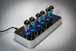
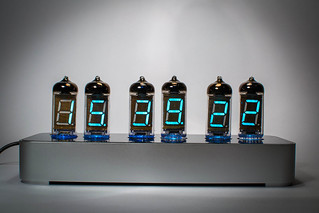
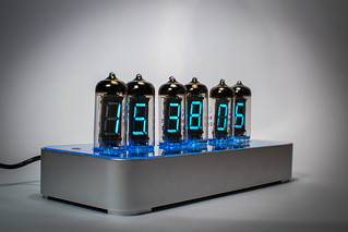
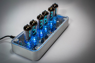
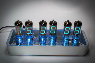
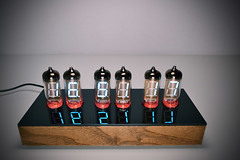
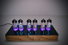
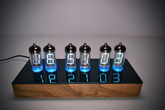
Under each tube there is an RGB LED filling in the tubes with more color and making them more impressive.

The tube segments are connected in parallel via the bus on MAX6921 and a FET is used to turn on/off the chip. Atmega168 is connected with ISP to MAX6921. A 32,768KHz crystal updates RTC seconds. Also a buzzer has been used for alarm mode and button press indication.
Why 32.768kHz?
Crystals with frequiency 32,768KHz is used in RTC's beacuse they make perfect division with numbers power of two including 128. 32768 / 128 = 256. If we use this crystal with a clock prescaler of 128 synchronizing an 8-bit counter the timer will reach it's max value and will trigger an overflow interrupt once per second with accuracy of 0.002% depending on crystal and ambient temperature. The counter overflow interrupt is then used to count Real Time Clock's seconds.
Construction
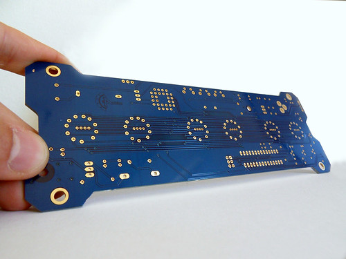
The clock's PCB
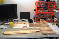
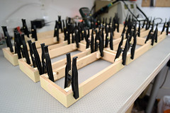
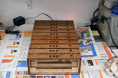
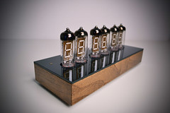
Wooden Case
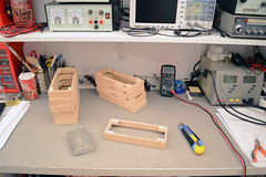
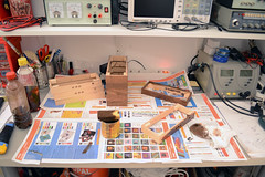
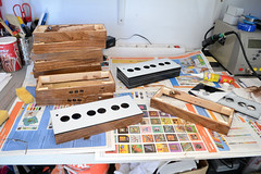
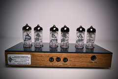
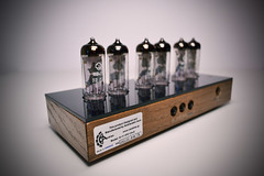
Test after soldering
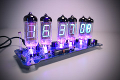
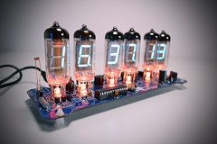
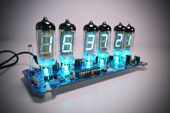
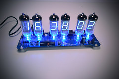
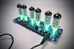
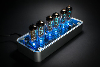
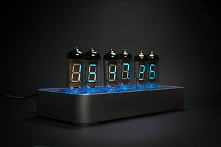
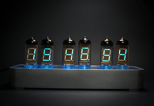
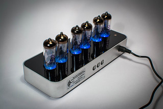
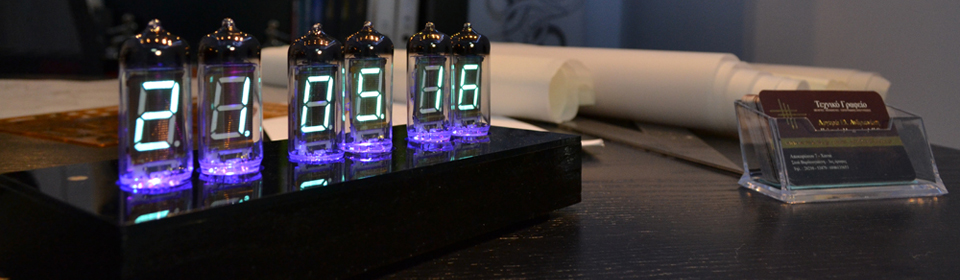
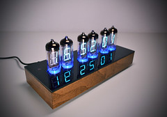
Fully Assembled
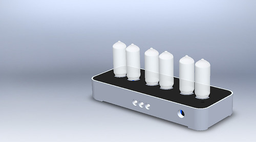
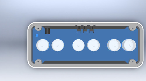
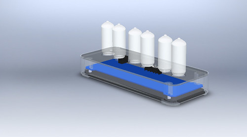
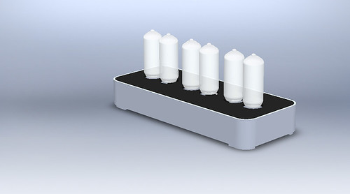
Preview
Wooden Case


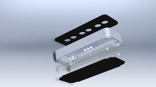
Aluminium 3D Model

Aluminium Real Model